
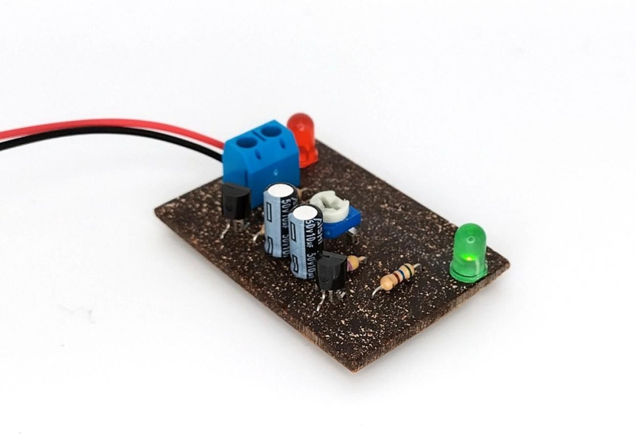
Instead of disposing of this biomass waste, the team processes it into a plastic-like material through an innovative process involving molding and air-drying, resulting in a small, approximately 0.5 cm thick plate with a density of 1.23 g/cm³, comparable to the density of conventional printed circuit boards (PCBs). Using direct ink writing or a standard etching process and manual soldering, the researchers were able to deposit electronic components directly onto the fungal plates.
Very cool … but in most cases, I wouldn’t want my circuit boards to be biodegradable. I’d be worried that a bit of accidental moisture or humidity exposure or something is going to leave my electronics rotting away on the inside and lead to premature failure.
Still, though, this could be very good and useful for more short-term or disposable type electronics … though the other components on the board certainly aren’t compostable, so ‘disposable electronics’ should still be something kept to an absolute minimum.
I wouldn’t want my circuit boards to be biodegradable
It’s true that in the article they do mention that the board needs to be optimized in terms of its water absorption. Still, this is a bioplastic, meaning it’s not like a cardboard or something that will start biodegrading on you out of nowhere.
Re “bioplastics” and similar technologies: people really underestimate what some of these types of things are capable of. There’s a pretty big spectrum between tissue paper that lasts days and thermoplastics that last centuries, but for some reason when people hear “biodegradable” anything they immediately think of the tissue paper. There’s still a long way to go in the material science (mostly in terms if economic viability) but some environmentally safe materials can be surprisingly robust.
PLA looks and feels like any other plastic. Pretty sure it lasts a very long time if you were to drop it on the floor of a forest and that is an ideal location for biodegrading.
Got a cheap 3D ages ago which is why I looked it up. Don’t really use it much though, said I would buy a better one if I use it but only used it like 3 times in a few years now.
IIRC, PLA just doesn’t biodegrade unless it’s exposed to high temperature. It’s “biodegradable” but only under specific conditions.
I would want burnable without toxic fumes over compostable. Toss it in a incinerator and collect the metals after.
Bioplastics is probably also a key to unlock that
this could be very good and useful for more short-term or disposable type electronics
The path to truly sustainable electronics is to reduce the disposable shit.
You shouldn’t be getting your electronics wet, anyway. Also, cardboard boxes last longer than my electronics in most cases.
This would work pretty good in most cases.
You shouldn’t be getting your electronics wet, anyway.
It’s to be avoided, sure. But sometimes accidents happen. Or sometimes it’s just really humid.
Given how many are out there, anyone making a compostable RFID chip should get a prize.
The coil should be fairly easy. Just find something that’s conductive and compostable.
The tiny silicone chip will be much harder to replace.
That’s neat. Do we also have compostable components? If so, we could have fully compostable devices. :D
If you can compost the board you can recover the components / metals more easily … maybe?
Do we also have compostable components?
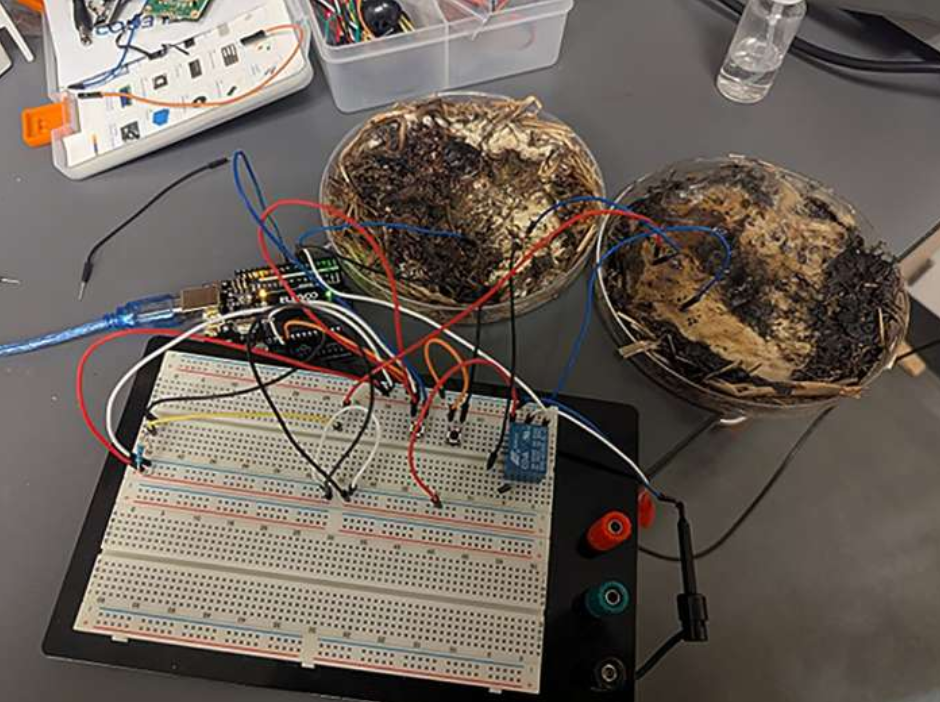
I know only a bit about bio-tech that comes from fungi, and people are working on it, but we’re not there yet to my understanding. As one example, researchers from The Ohio State University recently discovered that common edible fungi, such as shiitake mushrooms, can be grown and trained to act as organic memristors, a type of data processor that can remember past electrical states.
This one looks like that:
And here are some relevant articles, in case you feel like checking them out.
Are there use cases where it’s especially important for circuit boards to be compostable?
They’d be good for anything disposable that will be thrown into the trash
I guess the used vapes I find lying around have circuit boards in them
Yeah, but we could also ban vapes without replaceable batteries that cannot be charged.
There’s no reason for vapes to exist that are throwaway products.
Powerbanks can be charged. Vapes are just smaller powerbanks with a heating element.
I don’t know all the details, but the impression I get is that much of the popularity of disposable vapes has been driven by regulatory efforts to crack down on other aspects of vaping, even when the disposable vapes themselves are made illegal by them:
But Nancy Heredia-Villanueva, the mom who stormed the gas station, says local authorities in her area haven’t shown interest in enforcing sales of illegal vapes – even though they’re specifically banned in New Jersey law.
First, she reported the store to police: “I had to actually email ordinances to the detective,” she says. "And even then, he was like: ‘Well, what am I supposed to do about it?’
In general it seems like a complex issue with a variety of things behind it (at least one comment here implies that bans on taking vapes on planes also drives the use of disposables for instance), so if the goal is to address the e-waste part of the problem I could see how you might want a multi-pronged approach. But yeah compostable circuit boards isn’t really a total solution, those things also have lithium batteries etc.
I suppose it makes extracting the valuable/scarce materials easier when the circuit boards brick
When the PCB is sus 📮